Assembling, testing, modifying. These are things we do with PCBs every time we build them. This blog offers a few tips to design your board for ease of assembly, testing, and modification.
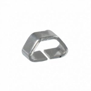
Put test points pretty much everywhere. Whether it’s a first spin or an eighth spin, lots of test points are a good idea. Make sure you have enough space to get a multimeter or scope probe into your test point without shorting anything. You can buy parts designed to make hooking a scope probe up to your circuit easier, like this one on Digi-Key:
Make vias large enough to stick a wire in it for testing. (I don’t bother for ground vias). Say you’ve designed your board, built and tested it, and you’re trying to hand-modify a circuit. Maybe you want to connect a trace on your board to an IC that you’ve dead-bugged onto your solder mask and you want to add a wire sticking off the board to make it easier to attach an oscilloscope. Connecting a wire to a trace is easier if you have an empty plated hole to solder your wire into. When manually adding wires to a board, I prefer to use solid-core wire with decently thermally tolerant insulation.
Although making it easy to solder in additional wires is great, if you can anticipate during design that there’s a chance that you will need to short two traces to each other after the board has been fabricated, lay down the footprint for a 0 Ω resistor and don’t populate it. In general, if you think something might be needed, it usually doesn’t hurt to put down the footprint for it. You may even want to put down a whole extra power supply.
Place 0 Ω resistors in series with everything you think will be useful to isolate during testing. It can be quite useful to isolate sub-circuits from the rest of the board to test them. One such subcircuit is a switched-mode power supply. It’s standard practice at StarFish to put a 0 Ω resistor at the output of a switched-mode power supply. The power supply can be tested without a load to ensure that the voltage is correct. This can be useful for other subcircuits as well.
Put signal traces on the outer layers rather than the mid layers for a prototype. When you modify the board, you’ll likely want to cut some traces somewhere in the process. This is why I try to keep signal layers on the outer layers of a PCB for the first few revisions of a board. Cutting a trace is going to be more difficult if the whole thing is buried in one of the mid layers. If you’re designing for production, burying traces in a mid layer with ground polygons on the top and bottom layers can provide shielding.
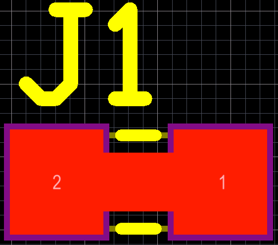
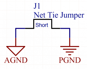
Net ties are great. In our Altium libraries at StarFish, we have net ties shaped like 0603, 0805, or 1206 resistors. I use them for traces that I want connected by default, but think there’s a chance that I’ll want to cut them. If I need the connection back, I can always solder a 0 Ω resistor right there.
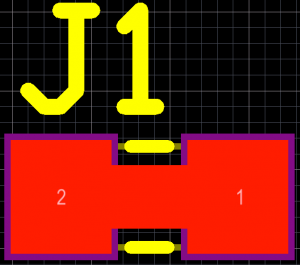
If you’re splitting your ground (for instance, one for digital and one for analog), net ties can also be a convenient way to show the connectivity on the schematic and ensure that components are grounded as desired.
Include thermal reliefs on pins that connect to your ground and/or power polygons. Thermal reliefs allow a large amount of heat to build up in the pad and melt the solder without heating the surrounding plane. Without thermal reliefs, the heat will escape and spread into the ground plane. It can be very annoying getting your solder to melt. In Altium, thermal reliefs are enabled by default. I always selectively disable them for vias. This is because I generally have ground polygons on all of my layers and add lots of stitching vias to keep the planes rock-solid. Below, you can see an example of ground pads that have thermal reliefs and stitching vias for the ground polygons without thermal reliefs.
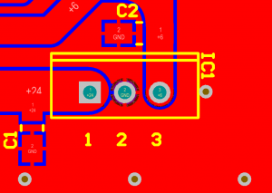
Rarely forgo thermal reliefs. It’s almost never a good idea. They are short enough that the additional resistance they add to the connection is very small. Being short also means that as they warm while current is passing through them, the ground plane to which they are connected serves as a heatsink and will usually keep them from getting too hot. If you forgo thermal reliefs, you may run into difficulty achieving a good solder joint.
For a PCB that had high current requirements, I once excluded thermal reliefs on a number of ground pads. To be safe, I checked with the board house and asked if foregoing thermal reliefs would cause issues. They said they could do it, but recommended a higher temperature rating for the FR4 to ensure the board could withstand the additional heat that would be required during assembly. This provided exceptional ground connections, but added cost to the PCB.
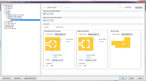
You can widen the thermal reliefs to achieve a balance between the electrical conductance of the connection and the ease of soldering. You can do this quite easily in Altium 17. In the PCB editor, go to Design → Rules. In the window that opens up, look under Design Rules → Plane → Polygon Connect Style → Polygon Connect (or whatever name you’ve given this rule). You can now set the conductor width of the thermal reliefs. Once you’ve set this, repour your polygons to see the result.
Through-hole components can make hand assembly easier. Appropriately sized surface-mount components are also easy (but not if you’re using 0201 resistors). QFNs are more challenging. Avoid designing BGAs into a PCB that is intended to be assembled by hand.
Minimize the number of different parts on the board. Don’t use a 10 kΩ 0603 resistor from Panasonic in one part of the board and a different 10 kΩ 0603 resistor from Yageo in another part of your board. For pull-up and pull-down resistors, you can often choose resistors that are already used elsewhere in your board since you often have a wide range of acceptable resistance values for these parts. Reducing part count has greater cost-reduction benefits when you get into larger volumes, but it also has benefits when you’re on the bench assembling your prototype.
Indicator LEDs can make testing and debugging more straightforward. They can be used to show when power rails are active or when key logic signals are in their high state. If there’s a microcontroller on the board, a couple of indicator LEDs connected to some of the output pins of the microcontroller can be a useful debugging tool during firmware development.
I hope you’ve enjoyed these design tips to make life easier during assembly, testing, and modification of your PCB. For more information on PCB Design best practices, check out these blogs from my colleague, Kenneth MacCallum. Happy routing!
Kristofor Dolberg is a StarFish Medical Electrical Engineer. This is his second blog on designing PCBs. Kris is a graduate of the University of Victoria where he was part of the ECOSat team that won first place in the Canadian Satellite Design Challenge.
