Maximizing Efficiency in a Switch Mode Power Supply
Why spend time maximizing efficiency in a switch mode power supply? Higher efficiency switching regulators get you more bang out of your buck. In a world of mobile devices, minimizing power consumption is a must. Don’t waste power in the power supply. This blog looks at the sources of inefficiency one would find in a typical buck or boost style DC-DC converter.
Primary Sources of Loss
The primary sources of loss in a switch mode power supply vary with different load currents. At high current the dominant source of loss is the power converted into heat across the resistance of the field-effect transistor (FET) and the inductor. At low current the dominant source is switching the FET on and off. The power required to switch the gate is constant at any load, but as more current is drawn by the load, the power used to switch the gate becomes a less significant portion of the total power converted.
Between heavy and light load is the sweet spot. This is where the effects of the gate switching power and the resistive losses are balanced and maximum efficiency is achieved. Ideally it is where the regulator will run, but that is determined by the amount of current drawn by the load. Compare your nominal current draw against the current draw for peak efficiency in the graphs provided in the converter’s datasheet. Optimize your DC-DC converter to be as close to these as possible. This will maximize efficiency for the variables inherent to the converter’s design.
Optimizing the FET
The requirements of the FET (voltage input, voltage output(s), the current draw, and effective power dissipation) will change for every design. There isn’t a perfect FET that will work for every application, but there are a few key criteria useful for maximizing efficiency.
Reduce the resistance between the Drain and Source (RDS) of the FET. RDS should be as low as possible, a 1Ω resistance at 2A becomes a 4W power loss, I aim for below 50mΩ as a rule of thumb for most applications. After you’ve done the math to determine the power loss, confirm that the FET or integrated circuit (IC) can effectively dissipate that power as heat. It is important to remember that as semiconductors heat up, the resistance will decrease. With the temperature leading to self heating, this could create a feedback loop and burn out the circuit.
Minimizing the gate charge (QG) will decrease switching losses in the FET by shortening the duration of the ID x VDS peaks that occur while the FET is switching. Even at heavy load where it’s not the dominant source of loss, it may still be worth reducing the gate switching loss. Remember, the voltage required for the FET to fully conduct will be higher than the advertised minimum turn on voltage. Consult the graphs in the FET datasheet to confirm the correct voltage for maximum conductivity. A lot of converter ICs have an integrated FET, and there may be no useful information on the VGS or CGSS.
Faster switching usually results in worse Electro Magnetic Compatibility (EMC), so be sure to employ strategies that reduce EMC. In high power situations the EMC could be much worse, it may be worth increasing R with a resistor to slow the switching even though it will result in lower efficiency.
Synchronous & Asynchronous Converters
Synchronous converters have a built-in low side switch in place of the rectifier diode used in an asynchronous converter. The synchronous converter will almost always be more efficient than the asynchronous. The power burned across the diode will dwarf that of the low side FET at any reasonable RDS (< 50mΩ).
In the case of asynchronous converters, Schottky diodes can be a good replacement for rectifier diodes. They have a significantly lower forward voltage drop. Schottkys have a slower reverse polarity recovery time, so be sure to use a frequency that will work for the Schottky. Luckily, lower frequencies are more efficient as they result in a lower inductor core loss and gate switching loss.
Inductor Considerations
Just like the FET, there is also power burned across the Resistance (DCR) of the inductor. Selecting an inductor with a small DCR is helpful in reducing power loss.
The physics of inductor switching loss is beyond the scope of this blog. There are many papers on the subject, but what you need to know is that core loss increases with the switching frequency. Higher switching frequencies allow for selection of physically smaller inductors. In your design, the choice could be a trade off between size and efficiency. If you have the space, a larger inductor with a lower switching frequency will minimize these losses. Choosing a converter IC with a lower or adjustable switching frequency allows for more control of these factors.
Be sure to simulate the inductor to ensure that the current won’t cause it to saturate.
Consult the Datasheets
Many datasheets now have efficiency graphs and recommended component values. Sometimes they even include recommended part numbers. The manufacturer has also worked to get the most out of their DC-DC converter. While it’s unlikely you will see the same results they achieved in their near ideal test environment, it is a good idea to use them as a starting point to check your numbers.
Conclusion
The main ways to increase efficiency in a Switch Mode Power Supply are:
- Read the datasheets and consult manufacturer reference designs
- Minimize the RDS of the FET and DCR of the inductor
- Consider using a synchronous converter when possible
- Identify the sweet spot frequency where the inductor should switch
Luke Mills is an Electrical Engineer. A graduate of the University of Victoria, Luke was an Electrical Lead of the UVic AERO team where he built an Avionics Stack that interfaces and controls all of the radios, GPS, autopilot, and control surfaces. This is Luke’s first StarFish Blog.
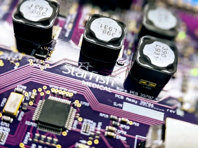
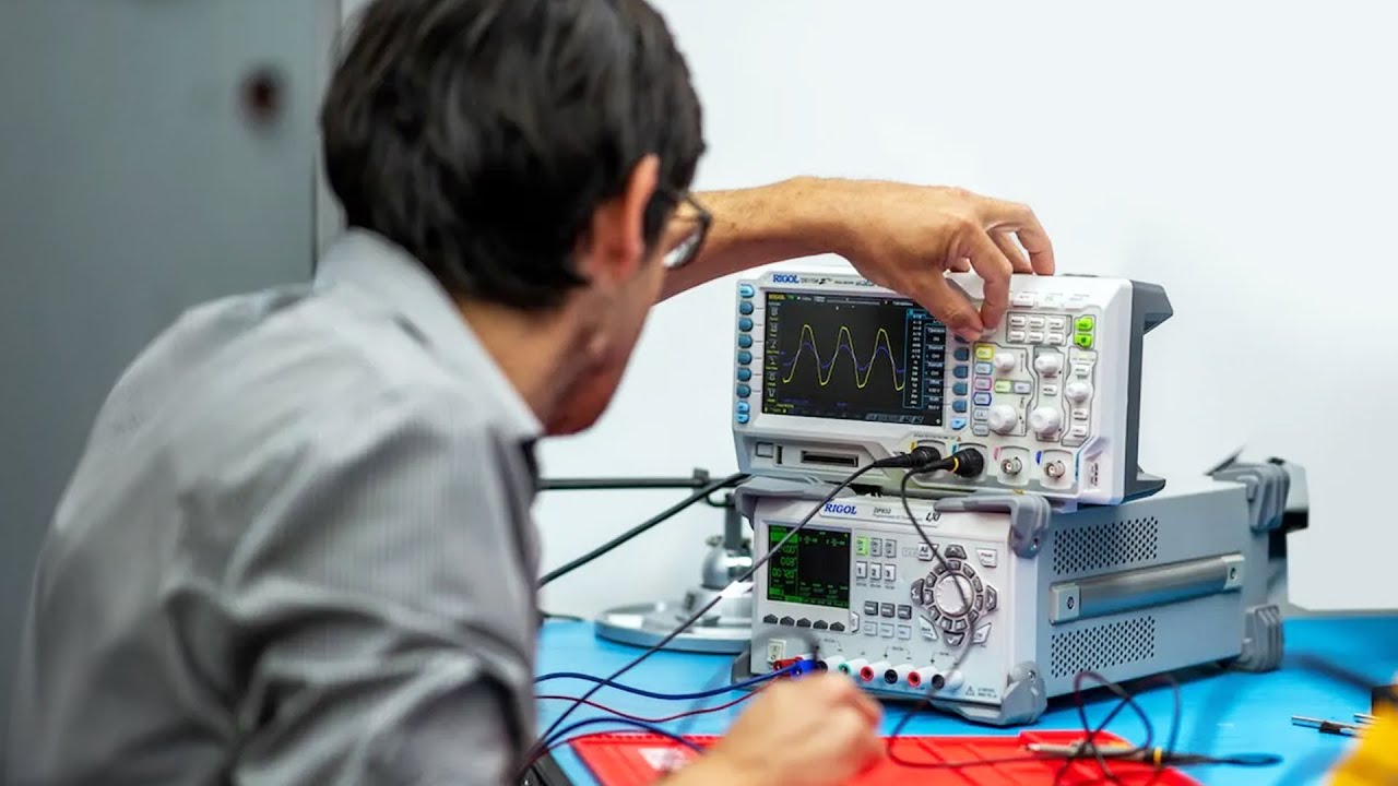
Images: StarFish Medical