Optical Detectors: An Overview
TL;DR
- Optical detectors are essential in medical devices that use light for diagnostics, monitoring, or therapy
- They measure photon energy rather than directly detecting optical frequencies
- Two main types exist: photothermal and photoelectric detectors
- Photothermal detectors measure temperature changes and are useful for energy measurement applications
- Photoelectric detectors convert light into electrical signals and are more commonly used in MedTech Photodiodes are the most widely used detector due to their sensitivity, speed, and wide operating range
“Accuracy of observation is equivalent to accuracy of thinking.” — Wallace Stevens, Adagia, Part One
Humans have been capturing visual stimuli in art for millenia. But the invention of photography in the late 19th century represented a revolution in more accurately memorializing the world around us. These days, electronic detection of light is the heart of any optical medical product – either in terms of providing raw data to drive or diagnose medical conditions, or verifying the effective and safe operation of a therapeutic device. Whether it be a pulse flow oximeter, an optical coherence tomography device, or a light-based therapy or surgical technology, electronic optical detectors are key to successful operation.
This blog reviews the main families of optical detectors and the major technologies in those families. Along the way, I’ll share some major use cases, advantages, and drawbacks of the different technologies, with a focus on non-imaging detectors (my colleague Ryan Field has discussed imaging detectors in previous blogs).
Although electric fields can be directly detected at lower frequencies, optical frequencies are too high to enable direct detection. Instead, optical sensors measure the energy contained in the electromagnetic field. This energy is proportional to the square of the electric-field strength – for this reason, such detectors are occasionally referred to as “square-law detectors.”
It’s worth noting the energy contained in a single photon, as given by Einstein’s relation E = hc/λ. In this expression, h is Planck’s constant, c the speed of light, and λ is the wavelength, ranging from ~200 nanometers for deep ultraviolet to 2500 nanometers for mid-infrared. The longer the wavelength, the lower the energy carried by each photon. When these numbers are put together, you get photon energies ranging from as much as 10−19 J to as little as 10−20 J for the wavelengths quoted above – quite a small number, indeed!
Generally, detecting single photons or small photon fluxes requires special technology. However, typical light sources tend to generate large numbers of photons per unit time, and there are multiple detector technologies for measuring continuous sources producing nanoWatts to tens of Watts of power, or pulsed sources producing picoJoules to tens of Joules per pulse (for moderate pulse repetition rates). Higher-power or higher-energy sources tend to be measured through judicious use of beam samplers or other optical attenuation to reduce photon flux on the detector itself.
There are two main families of non-imaging detectors:
- Photothermal
- Photoelectric
Photothermal Detectors
Photothermal detectors work by sensing the temperature change induced in a material by the light power/energy that is incident upon it. To understand the general magnitude of this temperature change, consider a continuous beam of green light (λ = 532 nm) of moderate optical power 100 μW (corresponding to an optical flux of ~3 ×10¹⁴ photons/second). If all that energy were absorbed in a thermally isolated detector with a typical heat capacity of, say, 310 μJ/K (typical of a pyroelectric sensor), then that would raise the detector temperature by 0.3°C/s. Because photothermal detectors respond only to deposited power/energy, they tend to work across a broad spectrum of incident wavelengths, limited only by any wavelength variation in their absorptive coatings.
There are three main photothermal technologies:
- Pyroelectic detectors are constructed of pyroelectric materials, which have a electric polarization that changes as their crystal structures respond to changes in temperature. This results in a changing charge distribution on opposite faces of the crystal. A dramatic example of this effect is seen in Figure 1. To serve as an optical detector, one face of pyroelectric material is covered in an optically absorbing material, while the other face is shielded from light. Once the temperature distribution of a pyroelectric material changes, the charge redistribution re-equilibrates in the face of nonzero material conductivity. For this reason, pyroelectric detectors only responds to the rate of change of temperature. Thus, they are suitable for quantifying pulsed light sources or chopped continuous sources. They are the preferred energy metrology for pulsed laser sources with pulse energies ranging from picoJoules to hundreds of Joules.
- Thermopile detectorsconsist of an absorber-coated surface and a cooled or constant-temperature surface, with a number of thermocouples connected electrically in series between these two surfaces. As the absorber surface heats up, a voltage difference of several microvolts to several volts is created and measured. Thermopile detectors are typically used to measure continuous powers ranging from microWatts to kiloWatts. Their response times are generally slow, though newer thin-film technology versions offer speedier response times (microseconds, rather than seconds).
- Bolometers are based on a material’s change in electrical conductivity with changing temperature. They are generally less sensitive than other detector technologies, but can be the detector of choice in the far-infrared or terahertz range. New, higher-sensitivity technologies operable at room temperature are on the horizon, using graphene or micro-mechanical technologies. On the very “high tech” end, cryogenic superconducting thin-wire bolometers that operate on the thermal edge of a superconductor/normal metal transition temperature can be sensitive at even the single photon level!
Photoelectric Detectors
The other main family of optical sensors relies on the creation of mobile charge carriers by the absorption of photons in a metal or, more usually, a semiconductor. These mobile charge carriers are then detected electrically. The main technologies in this second family of sensors are:
Photoemissive
In a photoemissive detector, a photon with energy greater than the work function of a metal liberates an electron from a metal electrode. The liberated photoelectrons are then detected electrically (Figure 2a).The canonical photoemissive detector is a photomultiplier tube (PMT), in which the liberated electron is accelerated into secondary electrodes by high voltages between the electrodes. As the electron collides with each subsequent electrode after acceleration, it liberates an “avalanche” of additional electrons, which are each multiplied when they collide with subsequent electrodes. In the end, the whole electron avalanche can then be detected as a current pulse. Photomultipliers are generally used to detect low fluxes of light and are even sensitive to single photons. At higher incident powers, they tend to saturate.
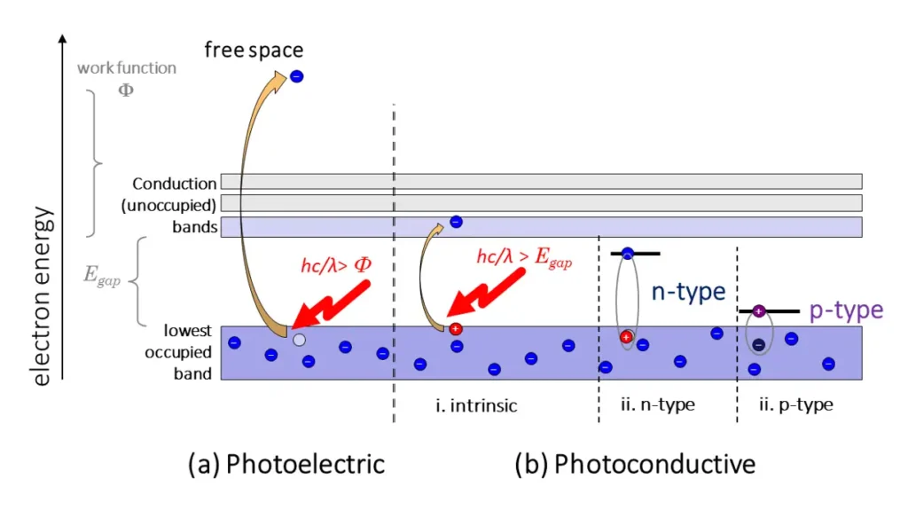
Figure 2. Non-diode photoelectric detector types. 2a. In a photoemissive detector, a photon with energy greater than the work function liberates an electron from a metal electrode through the photoelectric effect. This electron is then detected electronically – usually after avalanche multiplication; 2b. A photoconductive photon with energy greater than the band-gap energy of an undoped semiconductor creates extra charge carriers in higher-energy, partially filled conduction bands, thus increasing the conductivity of the material. This change in conductivity can be detected electronically. An n-type semiconductor is “doped” with atoms with more electrons than host (e.g. arsenic in silicon, allowing the detection of photons with lower energy than the semiconductor’s intrinsic band gap. Similarly, a p-type semiconductor is doped with atoms having fewer electrons than the host material (e.g. boron in silicon). In this case, the “missing” electrons in the crystal’s natural band structure create localized “electron traps,” leaving localized higher-energy holes in the band gap, allowing detection of lower-energy photons by the material’s change in conductivity. (Brian King, StarFish Medical)
Photoconductive
These detectors are made of semiconductor materials (Figure 2 b). The simplest implementation is with a pure (undoped) semiconductor. A photon with energy greater than the band-gap energy of an undoped semiconductor creates extra charge carriers in higher-energy, partially filled conduction bands, thus increasing the conductivity of the material. This change in conductivity can be detected electronically.
Alternatively, an n-type semiconductor may be used. Such a material is doped with atoms with more electrons per atom than the host (e.g. arsenic in silicon). The extra electrons don’t naturally fit into the crystal’s native band structure, creating localized defect levels in the band gap with excess negative charge. Thus, lower-energy photons are required to push electrons into the current-supporting conduction band.
Conversely, a p-type semiconductor is doped with atoms having fewer electrons per atom than the host material (e.g. boron in silicon). In this case, the missing electrons in the crystal’s natural band structure creates localized electron traps, leaving localized higher-energy holes in the band gap. The energy required to pull an electron away from the dopant’s excess positive charge and “fill” the hole in the conduction band is thus reduced – again, allowing detection of lower-energy photons by the change in conductivity.
In general, photoconductive detectors suffer from low sensitivity because the increased photoconduction charge can be obscured by thermally induced variations in photoconductivity. As well, they suffer from additional noise as the photon-induced charge carriers recombine.
Photodiodes
This third type of photoelectric detector is the most widely usedand is based on the physics of the junction between n-type and p-type doped semiconductors (Figure 3). As discussed above, n-type semiconductors have an excess of electrons due to electron-rich dopant impurities in the host semiconductor. Similarly, p-type semiconductors have a relative excess of holes due to electron-deficient dopant impurities.
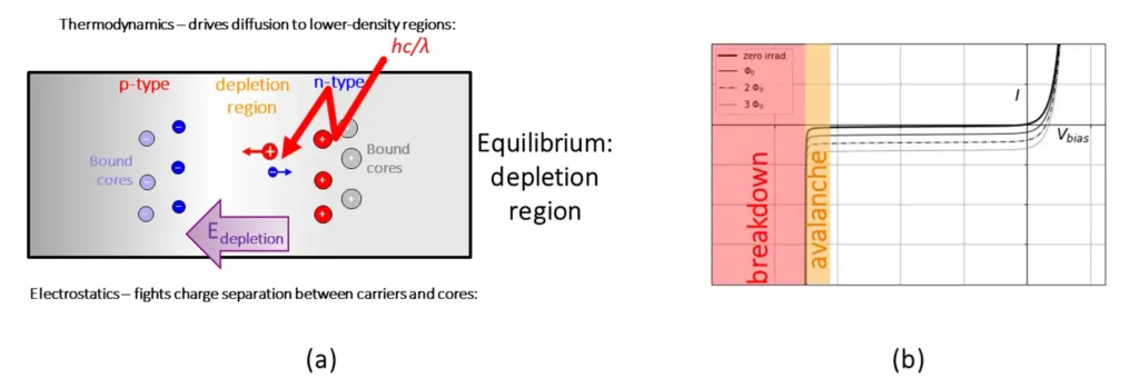
Figure 3a. Schematic diagram. The fundamental operation mechanism for a photodiode. At the junction between n- and p-type semiconductors, a depletion region is created, with a dearth of free conductors. This depletion region effectively serves as a capacitor, with relative excesses of negative and positive charge carriers at the opposite sides of the region, creating an electric field in the depletion region. Incident photons with energy greater than the band gap create electron/hole pairs, which generate a photocurrent as they are accelerated to opposite sides of the depletion region by the electric field. Figure 3b. Current vs. voltage curve for a photodiode, showing an overall offset dependent on the incident photon flux Φ. Photodiodes are typically operated at zero or negative bias voltages. (Brian King, StarFish Medical)
When an n-type and a p-type semiconductor are joined together, electrons and holes diffuse in opposite directions to the region with a deficit of each type of carrier. This leaves a free-carrier-poor depletion regionat the junction. Eventually, the buildup of opposite excess charge on opposite sides of this region sets up an electric field that halts the diffusion, and the junction reaches equilibrium. When a photon of sufficient energy falls into the depletion region, it creates localized electron-hole pairs. The depletion-zone electric field sweeps these charge carriers to opposite sides of the depletion zone, changing the charge distribution within the diode. The net impact of incident optical radiation, then, is to displace the current-voltage characteristic curve of the diode to more-negative current values (Figure 3b).This shift in the curve may be detected in two distinct manners of operation: the photovoltaic and photoconductive modes.
In photovoltaic mode, the photodiode is held at zero bias voltage. In the dark, the photodiode conducts only a small amount of “dark current” (due to thermally driven creation of conduction electrons) [1]. The advantage of photovoltaic mode is low dark current. However, as Figure 3bshows, the zero bias voltage point is very close to the “elbow” in the characteristic curve, so linearity between photon flux and photocurrent is generally not well-preserved with increasing photon flux.
In photoconductive mode, the photodiode is operated at negative bias voltage. This increases the linearity of response: indeed, in this operating regime (with careful choice of bias voltage and/or readout circuitry) the linearity can stretch over nine orders of magnitude (picoWatts to tens of milliWatts) [2].
Photodiodes are generally useful for detecting continuous or pulsed sources of light within the range of incident powers discussed in the preceding paragraph. For pulsed sources, the time-response of the readout circuitry must be considered carefully. One limiting factor is the parasitic capacitance of the photodiode depletion zone itself. In practice, the capacitance of the photodiode is reduced with increased negative bias voltage, which increases the width of the depletion zone and hence reduces the junction capacitance. (However, this increased bias voltage increases the so-called dark current: the current that flows through the diode in the absence of any incident light.) The capacitance is often further reduced by constructing the junction with an additional layer of low-doped intrinsic semiconductor between the n- and p-doped regions. Such a diode is referred to as a PINphotodiode.
At low photon energies (long wavelengths), the response of a given photodiode technology falls off as the photon energy drops below the band gap for that semiconductor. At higher energies, the photons tend to be absorbed by the substrate before penetrating to the depletion zone. The former challenge needs to be met by choosing a different semiconductor (e.g. indium-gallium-arsenide)![]() rather than silicon, for infrared wavelengths); the latter can be partially mitigated by specialized semiconductor architectures that move the depletion zone closer to the surface of the photodiode.
rather than silicon, for infrared wavelengths); the latter can be partially mitigated by specialized semiconductor architectures that move the depletion zone closer to the surface of the photodiode.
The above list covers the main technology families of optical detectors. Other technologies do exist (such as phototransistors, charge-injection devices, film, and even LEDs), but are not in common use – mainly due to performance or convenience defects compared to the above devices. Of the technology families discussed here, photothermal detectors are generally used either in calibrated energy meters (typically purchased from a dedicated supplier), or at infrared wavelengths, where the performance of the other technologies is limited. Photoconductive detectors should be avoided for most applications, due to their lower sensitivity and relatively higher noise levels.
In most medical-device applications, the optical detector will be a photodiode. Extracting the most performance from photodiode operation requires some care and attention, which I have not discussed in this brief survey. As well, I haven’t covered the operation of photodiodes in or near the “avalanche breakdown” regime at large reverse-bias voltages, where the operating mechanism is more akin to that of a photomultiplier tube. Stay tuned for deeper dives into these aspects of photodiode operation in future blog posts!
Brian King is Principal Optical Systems Engineer at StarFish Medical. Previously Manager of Optical Engineering and Systems Engineering at Cymer Semiconductor/ASML, Brian was an Assistant Professor at McMaster University. Brian holds a B.Sc in Mathematical Physics from SFU, and an M.S. and Ph.D. in Physics from the University of Colorado at Boulder. His research centered on implementing quantum information processing with trapped, laser cooled atoms – often single atoms confined in radiofrequency ion traps operating at ultrahigh vacuum.
Images: Adobe Stock
References
[1] This is essentially the mechanism by which solar cells work.
[2] It’s also worth noting that the inherent linearity of a photodiode also degrades at high current densities, on the order of tens of mW/cm². See, for example, https://qtwork.tudelft.nl/~schouten/linkload/phdiode.pdf, https://web.mit.edu/6.101/www/reference/Photodiode_Characteristics.pdf, or https://wp.optics.arizona.edu/jpalmer/wp-content/uploads/sites/65/2018/11/UDTapp_notes_02.pdf)
Figure 1
This video showing the temporary buildup of charge in a pyroelectric material in response to a dynamic change in temperature. In this example, the charge dissipates through dielectric breakdown in air between the top and bottom surface of the sample. In a pyroelectric detector, the charge buildup would be monitored (and dissipated) through a voltage or current sensor(https://www.infratec.eu/sensor-division/service-support/glossary/pyroelectric-detector/)
Related Resources

Ariana and Mark walk through what separates a clinical prototype from a proof-of-concept build, what determines how much testing and documentation you actually need, and where the regulatory line between significant risk and non-significant risk falls.

In this episode of Bio Break, Nick walks through both patent types after receiving two of his own in the mail, one of each, from the USPTO.

Scott Phillips sits down with Mickey Urdea to examine what actually distinguishes companies that reach commercial outcomes from those that do not.

Nigel Syrotuck breaks down the realistic medical device V&V cost and schedule for terminally sterilized devices, picking up after design freeze and walking through each major phase of the process.