Medical Device Miniaturization Options and Trade-Offs
Smart watches, near field tags, fitness trackers – everywhere you look, electronics are getting smaller. Medical device miniaturization is no exception, with many medical device manufacturers targeting very small form-factors for their devices. When miniaturizing a device’s electronics, there are several approaches.
At the simplest level, engineers can simply choose smaller parts, thereby shrinking the space taken up by the printed circuit board. Automated surface-mount assembly of parts such as QFN (quad flat no-lead) is a very common practice which does not significantly increase the assembly price of a PCB. Increasing the routing density is also an affordable option – many PCB houses now offer 375 micron width and spacing for a modest price bump, something which would have been enormously expensive a mere 15 years ago.
Pushing slightly farther, manufacturers offer components in CSP form factor (Chip-Scale Package). The devices are referred to as “chip-scale” as they are barely larger than the silicon dies packaged inside of them. These parts are available in ever-shrinking ball pitches – 0.4 mm is now common, and 0.3 mm devices are on the horizon. Low pin count devices can usually be accommodated on standard processes, provided there is enough routing space for fan out. Using high pin-count parts of this size requires moving to via-in-pad technology for PCB construction, which does add cost. X-ray or CT inspection of the finished PCBs is a must to assure good yields.
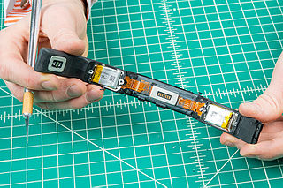
Flexible PCBs are all the rage now, and for good reason. Shrinking a rigid PCB by using smaller components with higher densities can only go so far. Enter flex PCBs. Flex PCBs are, as the name implies, circuit boards made out of flexible materials. Using a flex board allows the designer to contour the electronics to any available space inside of the device, permitting tight integration between the mechanical and electrical design. Flex boards have more benefits than just providing more surface area for PCB components. Flexible PCBs can replace interconnects usually formed by connectors and wiring harnesses in conventional designs. This saves space through the removal of bulky connectors, and greatly simplifies final assembly.
Just like regular PCBs, flexible PCBs can be made with multiple layers. So-called “flex-rigid” PCBs intermix flexible and rigid layers on the same board.
Join over 6000 medical device professionals who receive our engineering, regulatory and commercialization insights and tips every month.
Flexible PCBs do have a couple of drawbacks. The copper traces on flex PCBs are prone to cracking and tearing. This can be avoided by including proper design features such as tear stops and teardropped holes, and by following the IPC recommendations for minimum bend radius. Also, even though the board is flexible, the components most certainly aren’t. This can cause solder joint cracking unless the sections with components are stiffened. Stiffening is usually accomplished with an FR-4 sheet glued to the opposite side of the board. The number of bends, and particularly the number of back-and-forth bends, should be minimized when installing the board or breaking problems can occur. Engaging with the board house early on in the design process is critical to avoiding these problems.
Due to the higher amount of setup required by the manufacturer, flexible PCBs are more expensive to prototype with than rigid boards. For more complex designs, I recommend producing mock-up rigid PCBs first to test out all the electronics before ordering flexible PCBs. Provided that the timeline permits it, designing and building rigid mock-ups first can save costly flex re-spins down the line.
Further device miniaturization can be achieved through the use of custom integrated circuits. Designing a custom IC unshackles the designer from the restrictions of having to integrate functionality using off-the-shelf devices. This can be a very expensive endeavour, and is only worth it for devices expected to see very high volumes or which absolutely must meet miniaturization targets. If the high NRE costs can be overcome, however, it is possible to integrate almost all analog and digital functionality of a device onto a single die, potentially saving not just room for components but also room for interconnects.
Ultimately, a successful medical device miniaturization strategy must take into account the needs of the product. We now have the ability to make electronic devices smaller than ever before, but like everything in product design, the successful engineer must consider all the trade-offs.

Peter Kazakoff is a former StarFish Medical Electrical Engineer who worked on devices across many StarFish sectors. He graduated from the University of Victoria and this is his first of many blogs for StarFish.
Images: StarFish Medical