Medical Device PCB Design Tips – Design for Debugging
Getting a PCB (Printed Circuit Board) for a medical device right the first time is almost impossible. Datasheets can be misleading, or assumptions and architectures change. As a result, modifications are almost inevitable. Sometimes the modification is as simple as swapping resistors or adding capacitors. Other times it involves tacking on new circuits you had no idea you needed.
From my experience, accepting this eventuality and designing the PCB in a manner that allows for easy modification can be the difference between designing a functional prototype and a run of PCBs that are little more than paperweights.
This blog shares some of my medical device PCB design tips, learnings and suggestions, with the hope that it makes the debugging process a little less painful. For ease of reading, this blog is broken down into schematic and layout learnings/suggestions, with the understanding that the medical device design process can be quite fluid, often jumping between schematics and layout.
Schematics Tips
Net labeling
Carefully considering the labels of nets can avoid a lot of problems. Rather than leaving nets as pre-generated netlist names, Spend the time and label most, if not all nets on a schematic. This makes you think carefully about the function of each net, including logic levels, whether it is active high/low, etc. It is important to ensure labels are consistent with each other, i.e. inverted logic is all ~SIGNAL, or nSIGNAL, but not a mix of both. It may also be worth considering prefixes for digital voltage levels, if more than one exists in a design. This can help you catch where you need level conversion or inverters.
Reconfigurability, ease of modification
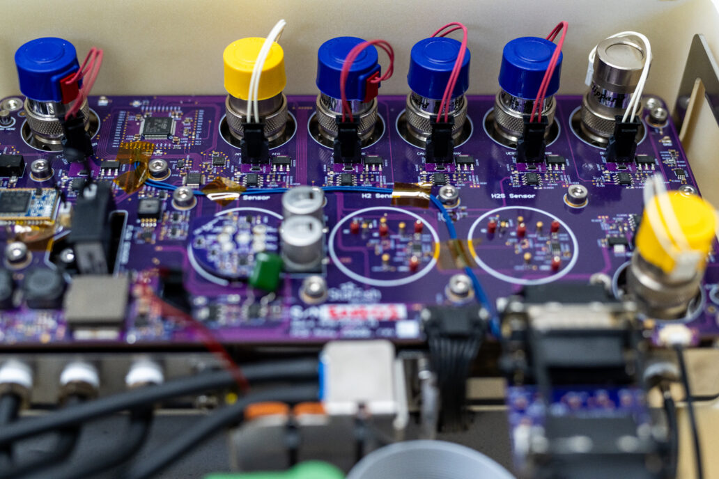
When designing a PCB with complex circuitry, you will likely be less confident in parts of the design. In these areas, including components such as 0-ohm resistors where you might need series resistance, matching networks, decoupling etc., can make implementing modifications much easier. This can be especially useful in UART busses, where TX/RX naming may be ambiguous at best.
Furthermore, breaking out unused pins to clearly labeled test points can make cutting and rerouting traces, or adding new circuits much more convenient. Lastly, including alternate circuitry that is not populated by default might mean you do not have to cut a single trace to modify a design.
Supplementary information
When working on schematics, it can be handy to include additional information (snippets from datasheets, charts, diagrams, equations etc), however it is not helpful to include the entire datasheet. It is a safe assumption that anyone who is debugging a PCB will have access to the design files of the board you’ve implemented, so transcribing every detail from every datasheet will only be confusing and hard to read. If there is a lot of information that absolutely must be included, consider transcribing values or equations into tables that are then placed on the schematic, or including extra documents with your design as reference.
Layout Tips
Placement of signal traces
Occasionally, it can be convenient to break out traces from an IC directly underneath it. I always strongly caution against this, unless it is unavoidable. This is because it can be quite challenging to remove the IC and reroute a trace running underneath if it was mis-connected.
Furthermore, I caution against running signal traces in internal layers, unless strictly necessary, or the density of a particular PCB calls for it. This is because it can be difficult to carefully cut down into internal layers to sever traces and reroute them. Lastly, unless a controlled impedance is required, I try to widen traces as much as reasonably possible to make cutting and soldering to traces much easier.
Component placement
When placing components, think about the scenario where you need to replace a component and how you might do it. Is there is room to bring in tweezers, a soldering iron, etc.? Some designs may not allow for strict adherence to this suggestion; however consideration of rework is always helpful. This is especially true when placing connectors, as they may have latches that swing open/closed, or bulky housings that could intersect other components.
Furthermore, I suggest choosing components appropriate to the density/signal speeds that your design needs. This is to avoid small components that may be challenging to rework. Generally, I try to go no smaller than 0402 for passives and avoid BGA’s unless unavoidable.
Text placement
Silkscreen can be a very valuable tool on a PCB if used correctly. It can be used to label jumpers, switches or LED functionality, or what a particular connector is supposed to mate to. I tend to use larger text with a solid background for connectors, and smaller text for individual component designators. The visual difference can make them easier to find. I also strongly suggest including meaningful labels next to connectors, switches and LEDs. On larger boards, putting borders around functional groups or schematic sheets with a large label nearby can help find subcircuits or individual components.
Summary
I hope my PCB design tips, schematic learnings and suggestions make the debugging process a little less painful. As I mentioned at the beginning of this article, the design process can be quite fluid, often jumping between schematics and layout. Getting a PCB (Printed Circuit Board) right the first time is almost impossible. Accepting this eventuality and designing the PCB in a manner that allows for easy modification is often the cleanest path to designing a functional medical device prototype.
Mike Ganzert is an Electronics Engineer at Starfish Medical. He received his Bachelor’s of Applied Science in Electrical Engineering from UBC Okanagan in 2021, with a focus in medical devices.
Image: StarFish Medical
Related Resources

Connected health devices are multiplying fast. We examine the gap between remote monitoring’s promise and its reality.

Ariana and Mark walk through what separates a clinical prototype from a proof-of-concept build, what determines how much testing and documentation you actually need, and where the regulatory line between significant risk and non-significant risk falls.

In this episode of Bio Break, Nick walks through both patent types after receiving two of his own in the mail, one of each, from the USPTO.

Scott Phillips sits down with Mickey Urdea to examine what actually distinguishes companies that reach commercial outcomes from those that do not.